Samsung’s roughly $260 million research commitment in Japan highlights the growing importance of connecting processors and memory.
The race to build faster, more efficient AI chips is making advanced packaging a bigger consideration for U.S. chipmakers and investors—a shift underscored by Samsung Electronics’ review of its Japanese packaging research operations on Nov. 1, 2026.
As AI systems demand more computing power, performance increasingly depends on how efficiently processors and memory exchange data. That puts greater weight on the materials, equipment and manufacturing processes used to connect chips, extending the investment stakes beyond the chips themselves.
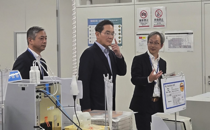
Samsung Chairman Lee Jae-yong visited the company’s Advanced Package Lab in Yokohama to review technology development and discuss cooperation with Japanese materials, components and equipment suppliers, the company said.
The visit reflects an industry challenge: Improving individual chips is only part of the task. Moving data between them quickly, while limiting power consumption and heat, is becoming essential to improving AI hardware.
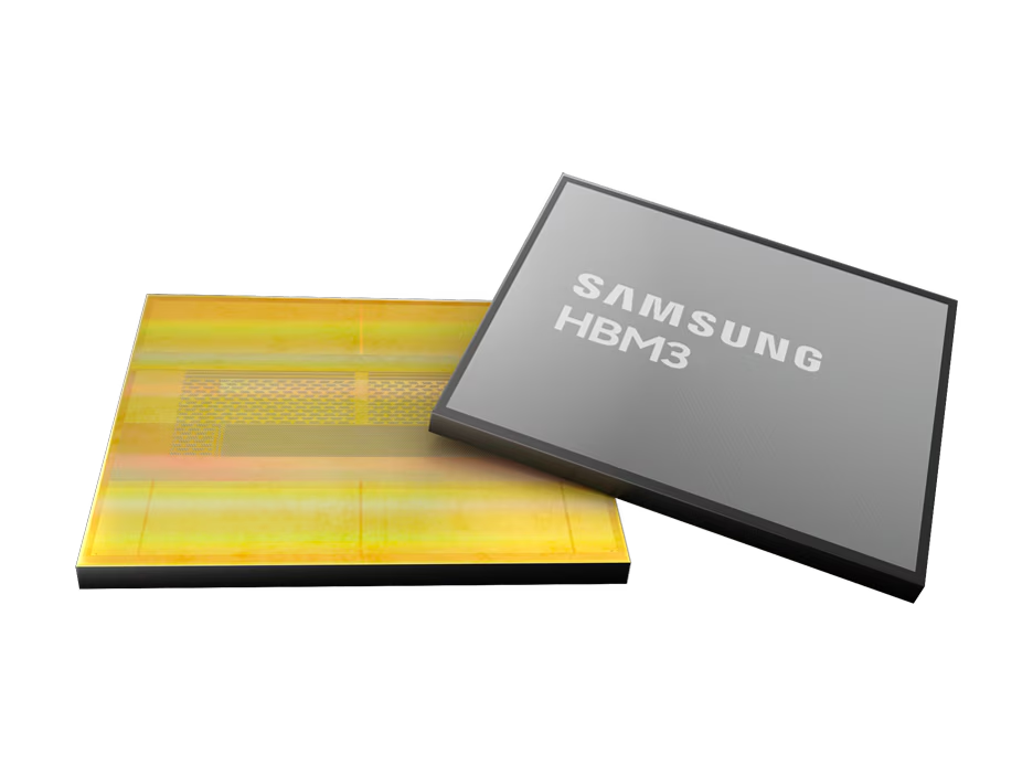
Advanced packaging addresses those constraints by bringing graphics processors and high-bandwidth memory together in a single package. The processors perform calculations, while the memory supplies the data they need. Better connections help those components operate more efficiently as a system.
For U.S. chipmakers and investors, the implications reach across the semiconductor supply chain. Progress in AI hardware depends partly on packaging capabilities—and on the suppliers that provide the specialized materials and equipment behind them.
Samsung established the Japanese lab, known as APL, in 2023 and committed approximately $260 million over five years beginning in 2024 to build its research infrastructure in Japan.
The company aims to pair its semiconductor design and manufacturing capabilities with Japanese suppliers’ expertise in materials and production equipment. The lab develops and evaluates packaging materials and processes, including technologies for precisely bonding semiconductor structures and using glass substrates in future chip packages.
Samsung also plans to broaden research into packaging architectures designed to deliver higher performance with lower power consumption.
Yokohama offers access to universities, research institutions and specialized engineers, alongside a concentration of materials and equipment companies. Samsung plans to expand its local research workforce and deepen cooperation with Japanese businesses and academic institutions.
The research effort complements Samsung’s manufacturing operations in South Korea. Lee visited the company’s Cheonan facility on June 23, 2026, to inspect operations that handle high-bandwidth memory and advanced packaging.
For the broader AI industry, the commercial test is whether advances in packaging can translate into faster systems, lower power requirements and reliable production at scale.