The race to build AI data centers is reshaping the semiconductor industry, pushing chipmakers to invest hundreds of billions of dollars in manufacturing capacity while developing new memory architectures to overcome data bottlenecks. For U.S. technology companies and investors, South Korea’s latest semiconductor announcements offer a window into two critical areas of competition: the scale of future chip production and the technologies needed to keep AI accelerators supplied with data as workloads shift toward inference.
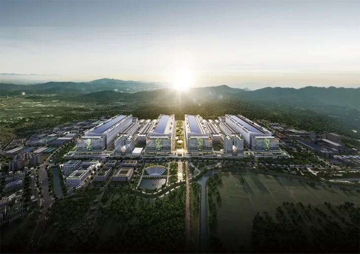
Samsung Electronics outlined its long-term manufacturing strategy on October 14, 2026, at South Korea’s Semiconductor Exhibition and Conference, unveiling plans for a semiconductor complex in Yongin backed by an investment of 360 trillion won, or approximately $257 billion at an illustrative exchange rate of 1,400 won per dollar. The project is intended to consolidate chip manufacturing, suppliers and design companies into a major production ecosystem as global demand for advanced semiconductors continues to grow.
Samsung plans to begin site development and construction of supporting infrastructure, including water and power facilities, in 2027. Its first fabrication plant is targeted to begin operations in October 2029, with six fabs planned for completion in Yongin by 2040.
The complex is expected to host about 70 companies, including suppliers of semiconductor materials, components and equipment, as well as fabless chip designers. Samsung also expects investment in transportation, roads and housing to support the surrounding economy.
For investors, the project represents a substantial long-term bet on advanced semiconductor manufacturing. Its commercial returns will depend on future demand, construction costs, production efficiency and the pace at which new chip technologies are adopted. The scale of the planned investment also highlights the importance of reliable electricity, water supplies and supplier networks in expanding semiconductor capacity.
Samsung used the exhibition to showcase technologies targeting the next generation of AI systems, including HBM4E, its seventh-generation high-bandwidth memory, and a base die for HBM4E manufactured using a 4-nanometer logic process. High-bandwidth memory, or HBM, stacks multiple memory layers to deliver data at high speeds to AI processors.
The company also displayed zHBM, a three-dimensional memory concept that stacks memory circuitry above a processor, and zNAND-O, a next-generation high-performance 3D NAND flash technology. These developments reflect a broader industry effort to improve data movement, memory density and system performance as AI models and computing workloads become more demanding.
SK Hynix, Samsung’s domestic rival and a major supplier of advanced memory, showcased HBM4E, high-bandwidth flash, or HBF, and enterprise solid-state drives. The company is working with SanDisk, Google and other technology partners to develop HBF as a potential complement to HBM.
The emerging technology addresses a growing challenge in AI infrastructure. While HBM delivers high bandwidth close to processors, AI inference can generate large volumes of data that increase demand for memory capacity. HBF is being developed to help supplement HBM where systems need to manage larger datasets, although its eventual role will depend on technical performance, system integration and commercial adoption.
Ahn Hyun, SK Hynix’s president and head of development, said during his keynote address on October 14 that HBM alone could struggle to accommodate the volumes of data generated during AI inference. He said the company had expanded its HBF development partnerships beyond SanDisk to include cloud service providers such as Google and companies developing AI accelerators.
SK Hynix aims to establish a final technical standard for HBF in January 2027, Ahn said. Standardization could help determine whether the technology gains broader industry support, but it does not guarantee immediate commercial deployment.
The developments illustrate how competition in AI semiconductors is expanding beyond the supply of high-performance processors. Chipmakers are investing in manufacturing capacity while exploring new combinations of memory technologies to reduce bottlenecks in increasingly complex AI systems.
For U.S. investors and data-center operators, the stakes extend across the semiconductor supply chain. Samsung’s planned manufacturing complex could strengthen South Korea’s role in advanced chip production, while SK Hynix’s HBF initiative could open another avenue for memory innovation. Both efforts face execution and adoption risks, but they underscore how infrastructure spending and memory architecture are becoming central to the economics of AI computing.